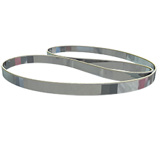
.jpg)
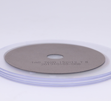
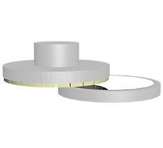
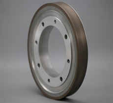
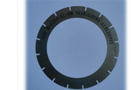
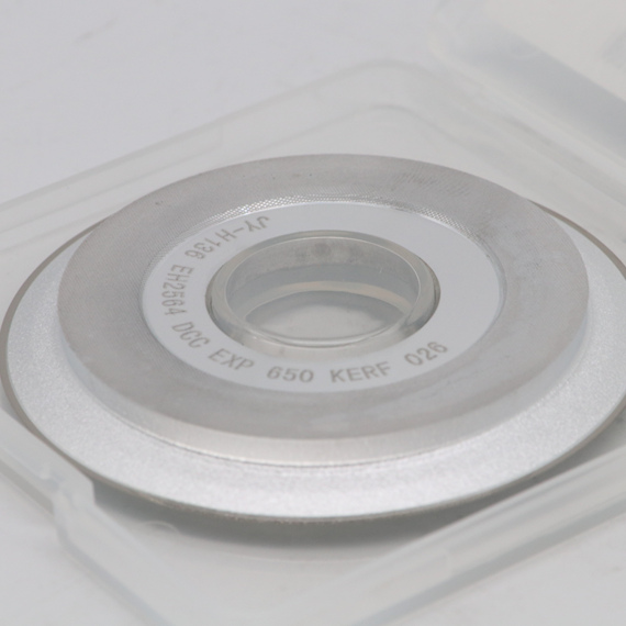
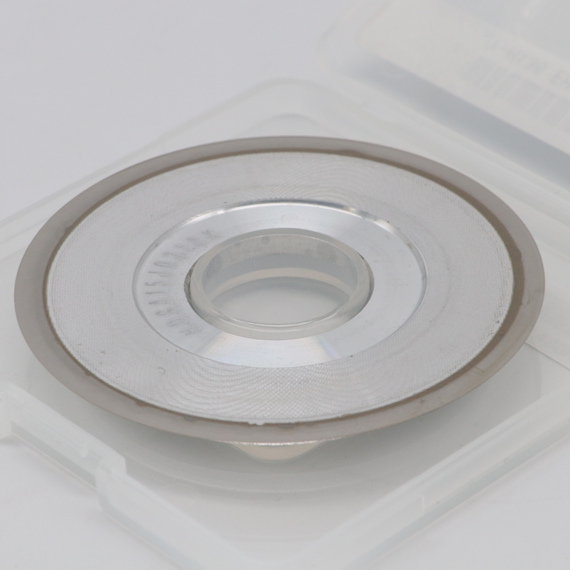
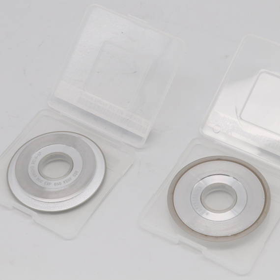
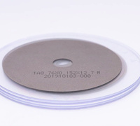
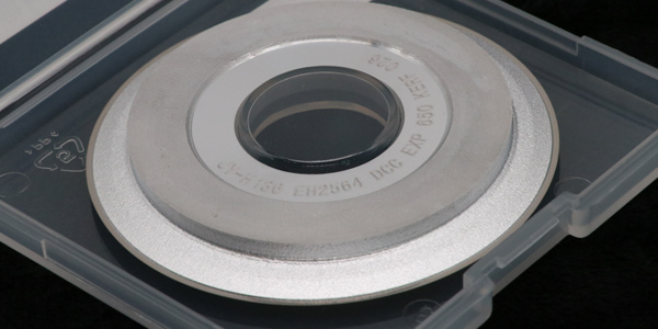 Performance advantages of electroplating diamond dicing blades (hub type)
• High toughness, high precision, ultra thin, good chip removal and cooling performance, long service life
• Can carry on the difficult angle cutting and the step cutting processing
• The use of imported diamond abrasive through the electroplating process and precision aluminum alloy flange forming.
• By adjusting the blades strength, can reduce the snake like cutting and blade damage
• The workpiece has no flying edge, burr residue and high yield
Applications of hub type electroformed diamond dicing blade
Scribing dicing IC wafers, gallium arsenide, gallium phosphide, epoxy resin board, alloy frame, ceramic substrate, composite board with interlayer, etc
.jpg)
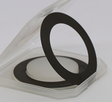
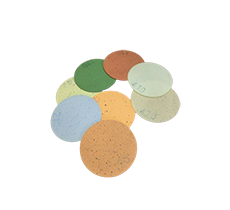
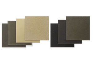
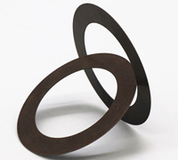
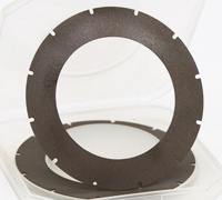
Dresser Board for dressing dicing blades
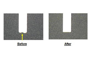
Dresser board is used for dressing and edged blade row, to increase sharpness, and reduce the chipping of the work piece, to reshape and perfect the blade edge to a flat edge
How to selection of the correct types of dicing blades to cut materials
* Binder of resin bond (soft strength) dicing blade, scribing hard and brittle material
* Binder of metal bond (medium strength) dicing blade
* Binder of electroplated bond (hard bond), scribing softer material


.jpg)

.jpg)
