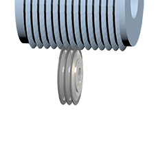
1. Technical Challenges in Semiconductor Wafer Dicing

Wafer dicing is a critical step in semiconductor packaging, separating dies from processed wafers. Driven by higher integration, power density, and larger wafer formats, third‑generation semiconductors (SiC, GaN) are rapidly growing. The industry faces key challenges:
- Extreme hardness & brittleness: SiC and GaN are far harder than silicon, risking chipping, microcracking, and breakage.
- Strict chipping control: Top chips require frontside chipping <10–30μm and backside <50–100μm.
- Narrow streets & high precision: Dicing streets shrink to tens of microns, demanding ultra‑thin, low‑runout blades.
- High abrasiveness: SiC/GaN wear diamond grains quickly, requiring premium diamond and durable bonds.
- Thermal & cooling risks: Insufficient cooling causes thermal stress; poor water quality leads to contamination.
- Sidewall quality: Defects reduce breakdown voltage for power devices.
Our core strategy: low chipping, long life, low thermal stress, high precision using fine graded diamonds, optimized resin/metal bonds, and tuned speed, feed, and DI water cooling.
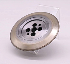
2. Custom Dicing Blade Design
We fully customize blades based on substrate type, wafer thickness, dicing street width, and dicing machine model.
Abrasive Selection
- Silicon wafers: D10–D20, standard grade, balanced life and chipping control.
- SiC / GaN: D3–D9, high‑strength narrow distribution diamond to minimize chipping.
- Ultra‑thin wafers: D3–D6, extra fine with soft bond for minimal damage.
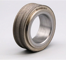
Bonding Systems
- Resin bond: Excellent self‑sharpening, gentle cutting, low chipping. Ideal for silicon and thin wafers.
- Metal bond (bronze base): High rigidity, long life, shape retention. Perfect for SiC, GaN, sapphire.
- Hybrid / layered bond: Roughing + finishing layers for superior entry/exit chipping control.
Key Specifications
| Material |
Grit |
Concentration |
Bond Hardness |
Blade Thickness |
| Standard Silicon |
D7–D20 |
50–75% |
Soft–Medium (K–M) |
15–40μm |
| SiC / GaN |
D3–D9 |
75–100% |
Medium–Hard (M–P) |
10–25μm |
| Ultra‑thin wafer |
D3–D6 |
25–50% |
Soft (J–L) |
10–20μm |
3. Process Parameter Optimization
Standard Silicon (200–300μm)
- Spindle speed: 30,000–40,000 r/min
- Feed rate: 30–80 mm/s
- Cut depth: wafer thickness +20–30μm
- Coolant: DI water + rust inhibitor
- Target: Front chipping <20μm, back <50μm
SiC Wafer (150–200μm)
- Spindle speed: 25,000–35,000 r/min
- Feed rate: 5–20 mm/s
- Cut depth: +30–40μm
- Coolant: High‑pressure DI water
- Target: Front <15μm, back <60μm
GaN‑on‑SiC
- Spindle speed: 30,000–40,000 r/min
- Feed rate: 3–10 mm/s
- 2‑step cutting (score + break)
- Filtered DI water
- Target: No delamination, minimal chipping
4. Cooling & Chipping Control
- Use 18.2MΩ·cm DI water to avoid contamination.
- Dual nozzles, 1–3L/min, 2–5bar to flush hard particles.
- Monitor chipping under high‑magnification microscope.
- Inspect groove uniformity for blade wear.
5. Blade Life & Dressing
- Resin blades: self‑sharpening.
- Metal blades: periodic dressing required.
- Measure life by total cutting length.
- Replace when chipping nears limit or current rises.
6. Recommended Process Roadmap

| Material |
Recommended Blade |
Core Strategy |
Quality Goal |
| Standard Silicon |
Resin D10–D20 |
Medium speed, high efficiency |
Chipping <20μm |
| SiC |
Metal D3–D6 |
Low speed + high pressure cooling |
Chipping <15μm |
| GaN‑on‑SiC |
Hybrid D3–D6 |
Step cut, ultra‑low feed |
No delamination |
| Thin Si <100μm |
Resin D3–D7 |
Low speed + adhesive tape |
Front <10μm |