1. Industry Background & Core Processing Pain Points in Display & Semiconductor Manufacturing
Global LCD, OLED and semiconductor manufacturing factories operate strict cleanroom production environments with zero tolerance for micro-defects on color filter (CF) substrates, optical glass and semiconductor wafers. During the color filter coating, exposure and development stages of LCD panel production, tiny foreign particle protrusions, coating unevenness, micro scratches and surface bumps frequently form on CF glass panels. These subtle defects directly cause pixel light leakage, color distortion, display spot failures and massive product scrap losses if left uncorrected.
Traditional rough polishing sheets, loose abrasive slurries and low-quality abrasive tapes cannot satisfy ultra-fine CF repair requirements: they generate excess micro dust, cause localized over-grinding that damages intact color filter layers, feature inconsistent substrate thickness leading to unstable polishing removal rates, and produce jagged cutting edges that introduce secondary particulate contamination into Class 100/1000 cleanrooms.
Our CF ultra-precision polishing tape is purpose-engineered exclusively to resolve all critical defect repair bottlenecks in color filter manufacturing and high-end optical/semiconductor polishing workflows. This premium abrasive film integrates uniform micron-grade alumina abrasives, high-purity polymer adhesive and flat PET base film via precision coating technology, delivering stable, low-damage surface modification without introducing secondary contamination for cleanroom mass production.
2. Product Manufacturing Composition & Technical Structure
Our CF ultra-precision polishing tape is fabricated through multi-step precision coating and slitting processes under dust-free cleanroom conditions, with three core structural layers that determine stable polishing performance:
2.1 Base Substrate: High-Flatness PET Polyester Film
We select high-transparency, ultra-flat biaxially oriented PET polyester film as the base carrier layer. The PET substrate undergoes strict thickness calibration during production, with total thickness tolerance controlled within micrometer range. This rigid, dimensionally stable base eliminates uneven tape deformation during high-speed polishing, prevents uneven abrasive grain contact with CF panels, and ensures uniform stock removal across the entire polishing contact area. Custom backing options are available to match diverse polishing machine fixtures: pressure-sensitive adhesive backing for fixed roller polishing equipment, and micro-fleece soft backing for flexible surface contact on curved optical components.
2.2 Functional Coating Layer: Uniform Alumina Abrasive & High-Purity Polymer Adhesive
The core polishing functional layer mixes fine alumina (AO) micro-abrasives with low-ion, low-outgassing novel polymer adhesive resin. Advanced high-speed dispersion equipment evenly distributes micron alumina grains across the PET film surface to avoid abrasive agglomeration, which is the root cause of micro-scratches on delicate color filter photoresist layers. The polymer adhesive formula is customized for cleanroom standards, featuring low dust shedding, chemical compatibility with CF photoresist materials, and stable bonding strength to prevent abrasive grain shedding during continuous polishing cycles.
2.3 Precision Slitting Process for Clean Edge Quality
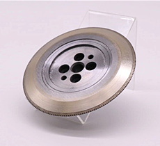
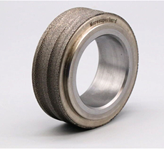
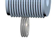
All finished polishing rolls are cut via ultra-sharp diamond slitting blades in dust-free workshop zones. The slitting technology eliminates burrs, loose abrasive fragments and edge powder, delivering smooth, particle-free tape edges that comply with strict semiconductor and display cleanroom particulate control regulations. No secondary dust pollution occurs during automatic tape feeding on CF repair polishing machines.
3. Complete Product Parameter Specifications
We provide standardized abrasive grit sizes, roll dimensions and backing styles to cover all mainstream CF defect repair and optical polishing processes:
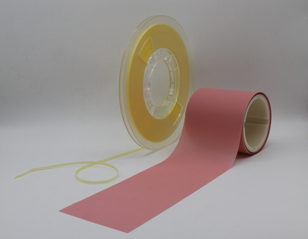
- Abrasive Material: High-purity alumina (AO) micro powder
- Available Grit Sizes for Tiered Finishing:
- 0.5μm ultra-fine grit: Final mirror finishing, removing ultra-tiny nano-scale CF protrusions without damaging thin photoresist coating
- 1μm medium fine grit: Universal defect repair for standard foreign particle bumps on mass-production color filters
- 3μm coarse fine grit: Rapid removal of larger coating protrusions and thick surface irregularities, reserved for pre-repair leveling
- Standard Roll Dimensions for Automated Polishing Equipment:
- Small narrow rolls: 50M length × 3.8mm width, matching small compact CF repair polishing machines for laboratory and small-batch production
- Wide long rolls: 100M length × 12.6mm width, optimized for large-scale continuous automatic polishing lines in panel mega-factories
- Substrate & Backing Options: Base material: High-stability PET polyester film Optional backing: Single-sided adhesive backing, soft micro-fleece backing (custom composite structures supported for special machine models)
4. Core Product Performance Advantages for Cleanroom Precision Polishing
Compared with generic domestic and imported abrasive polishing films, our CF ultra-precision polishing tape carries four exclusive technical strengths tailored for display and semiconductor high-cleanliness workshops:
4.1 Ultra-High Surface Flatness for Uniform, Controllable Polishing Removal
The rigid PET base film and evenly distributed abrasive coating eliminate uneven surface bumps on the tape itself. During CF panel repair, the tape maintains consistent contact pressure across the workpiece surface, effectively avoiding localized over-grinding that erodes intact red/green/blue photoresist layers and causes color filter scrapping. Manufacturers achieve highly repeatable polishing removal depth for standardized mass production quality control.
4.2 Superior Whole-Roll Thickness Consistency for Stable Process Repeatability
Every production batch undergoes full-length thickness online inspection during coating and slitting. Precise thickness tolerance across the entire roll length ensures identical polishing removal efficiency from the start to the end of each tape roll. This consistency eliminates frequent process parameter adjustments for workshop operators, drastically improving production line reliability and reducing manual testing downtime.
4.3 Burr-Free, Dust-Free Precision Slitting for Class 100/1000 Cleanroom Compliance
Conventional abrasive tape slitting produces plastic burrs and loose abrasive powder that contaminate CF glass substrates, triggering secondary pixel defects. Our diamond-blade clean slitting process delivers perfectly smooth tape edges with zero particulate shedding. The low-dust material formula meets strict cleanroom particulate emission standards, eliminating costly contamination-related rejects in high-end LCD and semiconductor production lines.
4.4 Low-Damage Micron Alumina Abrasive Formula for Delicate CF Photoresist Layers
Sharp yet uniform alumina micro grains perform gentle planarization rather than aggressive cutting. The optimized grain distribution suppresses deep micro-scratches on fragile color filter photoresist coatings, successfully repairing surface protrusions while fully preserving the original color filter optical performance, transmittance and color uniformity.
5. Main Industrial Application Scenarios
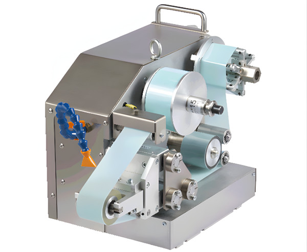
Our CF ultra-precision polishing tape is a core consumable for three high-tech precision manufacturing sectors with strict surface finishing requirements:
5.1 LCD Panel Color Filter (CF) Defect Repair (Primary Application)
This polishing tape is the standard consumable for automatic CF repair machines in LCD and OLED display factories. It targets common CF surface defects including foreign particle protrusions, coating uneven bumps, minor surface stacking flaws and micro height differences formed during photoresist coating, exposure and development. It restores flat, defect-free CF glass panels to qualified standards without damaging the thin color photoresist layers, significantly boosting CF finished product yield and reducing raw material waste.
5.2 High-Precision Optical Component Surface Finishing
Applicable for fine polishing of optical glass lenses, optical filters, sapphire optical substrates and precision glass light guide plates. The ultra-fine grit variants achieve ultra-smooth optical surfaces, eliminating micro height errors that distort light transmission and imaging performance for optical instruments, camera modules and display backlight components.
5.3 Semiconductor Industry Fine Precision Polishing Processes
Widely used for micro planarization of semiconductor auxiliary optical parts, wafer carrier glass and precision packaging optical components under cleanroom environments. The low-outgassing, low-dust material formula avoids ionic contamination that impacts semiconductor electrical performance, fully matching strict semiconductor manufacturing material access standards.
6. Operating Recommendations for Maximum Service Life & Repair Quality
- Grit Size Matching Rules: Use 3μm grit for large protrusion pre-leveling, 1μm grit for universal standard defect repair, and 0.5μm grit for ultra-fine final surface homogenization to prevent over-polishing of CF photoresist.
- Cleanroom Storage Requirements: Store unused polishing tape rolls in sealed dust-proof packaging under constant temperature & humidity to avoid surface adsorption of floating particles before use.
- Machine Fixture Matching: Select adhesive backing tape for rigid roller polishing equipment, fleece backing tape for flexible contact polishing machines to optimize surface conformity on uneven CF panels.
- Continuous Use Control: Replace tape rolls in time when abrasive grain shedding or uneven polishing marks appear on CF workpieces to prevent batch secondary defect generation.
7. Conclusion
For display and semiconductor manufacturers struggling with low CF repair yield, excessive cleanroom particulate contamination, unstable polishing removal rates and irreversible photoresist damage from ordinary abrasive tapes, our CF ultra-precision alumina polishing tape delivers a high-cleanliness, repeatable, low-damage defect correction solution. We supply standard 50M×3.8mm and 100M×12.6mm PET polishing rolls with customizable adhesive/fleece backing and three micron grit options (0.5μm / 1μm / 3μm) to fit all mainstream automatic CF repair polishing equipment.
Our technical team provides free sample testing and customized size slitting services for global LCD, optical and semiconductor production plants. If your workshop faces persistent color filter surface defect scrap losses or cleanroom particulate pollution issues, contact our international sales team to obtain tailored precision polishing tape solutions and boost your finished product yield.